|
|
|

|
|
|
|
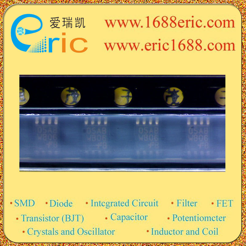
NC7WB3306K8X WB06 的参数 |
| 类型
Type |
总线开关 Bus Switch |
| 电路
Circuit |
1 x 1:1 |
| 独立电路
Independent Circuits |
2 |
| 输出高,低电流
Current - Output High, Low |
|
| 单电源
Voltage Supply Source |
单电源 Single Supply |
| 电源电压
Voltage - Supply |
4 V ~ 5.5 V |
| Description & Applications |
The NC7WB3306 is a 2-bit ultra high-speed CMOS FET bus switch with TTL-compatible active LOW control inputs. The low On Resistance of the switch allows inputs to be connected to outputs with minimal propagation delay and without generating additional ground bounce noise. The device is organized as a 2-bit switch with independent bus enable (OE) controls. When OE is LOW, the switch is ON and Port A is connected to Port B. When OE is HIGH, the switch is OPEN and a high-impedance state exists between the two ports. Control inputs tolerate voltages up to 5.5V independent of VCC. Space saving US8 surface mount package MicroPakTM? leadless package Typical 3? switch resistance at 5.0V VCC Minimal propagation delay through the switch Power down high impedance input/output Zero bounce in flow through mode. TTL compatible active LOW control inputs Control inputs are overvoltage tolerant |
| 描述与应用 |
NC7WB3306是一个2位的超高速CMOS FET总线开关与TTL兼容的低电平控制输入。低导通电阻的开关允许以最小的传播延迟和不产生额外的接地反弹噪声输入连接到输出。该设备被组织作为一个独立的总线启用(OE)控制的2位开关。当OE为低电平时,开关导通和端口连接到端口B,当OE为高电平时,开关打开和高阻抗状态之间存在着两个端口。控制耐输入电压高达5.5V,独立于VCC。 US8表面贴装封装节省空间 MicroPakTM无铅封装 典型3Ω开关电阻,在5.0V VCC时 最小的传播延迟通过开关 断电高阻抗输入/输出 流经零反弹模式 TTL兼容的低电平控制输入 控制输入过压容限 |
| 技术文档PDF下载 |
在线阅读  |
|
|
|
|
|
相关型号列表 |
| 型号 |
标记/丝印/代码 |
厂家 |
批号 |
封装 |
数量 |
描述 |
详细资料 |
| NC7WB3306K8X |
WB06 |
FAIRCHILD |
00+ |
VFSOP8/US8 |
27000 |
集成电路ICIntegrated Circuit(IC)-逻辑电路Logic circuit-解码器、多路复用器、信号开关Signal Switch, Multiplexer, Decoder |
查看 |
|
|
|

