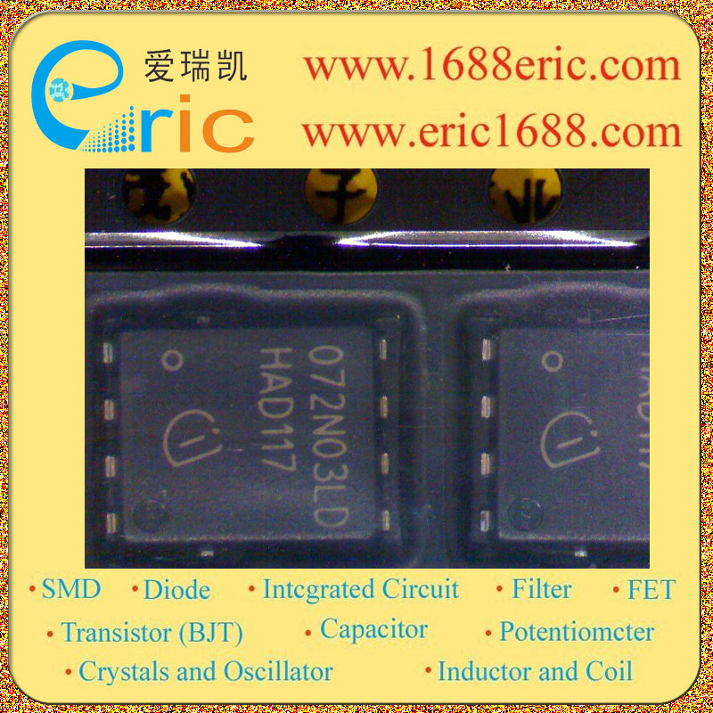
BSC072N03LDG 072N03LD 的参数 |
| 最大源漏极电压Vds
Drain-Source Voltage |
30V |
| 最大栅源极电压Vgs(±)
Gate-Source Voltage |
20V |
| 最大漏极电流Id
Drain Current |
20A |
| 源漏极导通电阻Rds
Drain-Source On-State Resistance |
7.2m?@ VGS = 10V,ID = 20A |
| 开启电压Vgs(th)
Gate-Source Threshold Voltage |
1~1.22 |
| 耗散功率Pd
Power Dissipation |
57W |
| Description & Applications |
Features ? Dual N-channel, logic level ? Fast switching MOSFETs for SMPS ? Optimized technology for DC/DC converters ? Qualified according to JEDEC for target applications ? Excellent gate charge product ? Very low on-resistance R DS(on) ? Superior thermal resistance ? 100% avalanche tested ? Pb-free plating; RoHS compliant ? Halogen-free according to IEC61249-2-21 |
| 描述与应用 |
特点 ?双N沟道逻辑电平 ?快速开关MOSFET的开关电源 ?优化技术的DC / DC转换器 ?符合JEDEC为目标的应用程序 ?优秀的栅极电荷乘积 ?非常低的导通电阻R DS(ON) ?卓越的热电阻 ?100%雪崩测试 ?无铅电镀,符合RoHS标准 ?无卤素根据IEC61249-2-21 |
| 技术文档PDF下载 |
在线阅读  |