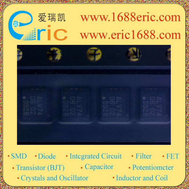
74ALVC74BQ ALV74 的参数 |
| 功能
Function |
设置(预设)和复位 Set(Preset) and Reset |
| 类型
Type |
D型 D-Type |
| 输出类型
Output Type |
差分 Differential |
| 元件数
Number of Elements |
2 |
| 每元件位数
Number of Bits per Element |
1 |
| 时钟频率
Frequency - Clock |
275MHz |
| 传播延迟时间
Delay Time - Propagation |
3.7ns |
|
正边沿 Positive Edge |
| 触发器类型
Trigger Type |
24mA,24mA |
| 输出高电平,低电平电流
Current - Output High, Low |
1.65 V ~ 3.6 V |
| 电源电压
Voltage - Supply |
Dual D-type ?ip-?op with set and reset;positive-edge trigger DESCRIPTION The 74ALVC74 is a dual positive-edge triggered, D-type flip-flop with individual data (D), clock (CP), set (SD) and reset (RD) inputs and complementary Q and Q outputs. The set and reset are asynchronous active LOW inputs and operate independently of the clock input. Information on the data input is transferred to the Q output on the LOW-to-HIGH transition of the clock pulse. The D inputs must be stable one set-up time prior to the LOW-to-HIGH clock transition for predictable operation. Schmitt-trigger action in the clock input makes the circuit highly tolerant to slower clock rise and fall times. FEATURES ? Wide supply voltage range from 1.65 to 3.6 V ? Complies with JEDEC standard: JESD8-7 (1.65 to 1.95 V) JESD8-5 (2.3 to 2.7 V) JESD8B/JESD36 (2.7 to 3.6 V). ? 3.6 V tolerant inputs/outputs ? CMOS low power consumption ? Direct interface with TTL levels (2.7 to 3.6 V) ? Power-down mode ? Latch-up performance exceeds 250 mA ? ESD protection: HBM EIA/JESD22-A114-A exceeds 2000 V MM EIA/JESD22-A115-A exceeds 200 V. |
| Description & Applications |
双D型触发器触发器置位和复位;正边沿触发 说明 74ALVC74是一个双正边沿触发,D型 个人数据(D),时钟(CP),集(SD)和触发器 复位(RD)输入和互补Q和Q输出。 置位和复位是异步的低电平输入 并独立运作的时钟输入。信息 输入的数据被传输到的Q输出端上的 LOW-to-HIGH过渡的时钟脉冲。 D输入 必须是稳定的一个建立时间之前,在LOW-to-HIGH 时钟转换为可预见的操作。 施密特触发器的时钟输入的行动,使电路 高度耐慢时钟上升和下降时间。 ?宽电源电压范围从1.65到3.6 V ?符合JEDEC标准: JESD8-7(1.65?1.95 V) JESD8-5(2.3到2.7 V) JESD8B/JESD36(2.7至3.6 V)。 ?3.6 V宽容输入/输出 ?CMOS低功耗 ?直接接口TTL水平(2.7?3.6 V) ?掉电模式 ?闭锁性能超过250 mA ?ESD保护: HBM EIA/JESD22-A114-A超过2000 V MM EIA/JESD22-A115-A超过200 V |
| 描述与应用 |
|
| 技术文档PDF下载 |
在线阅读  |