|
|
|
|
|
|
|
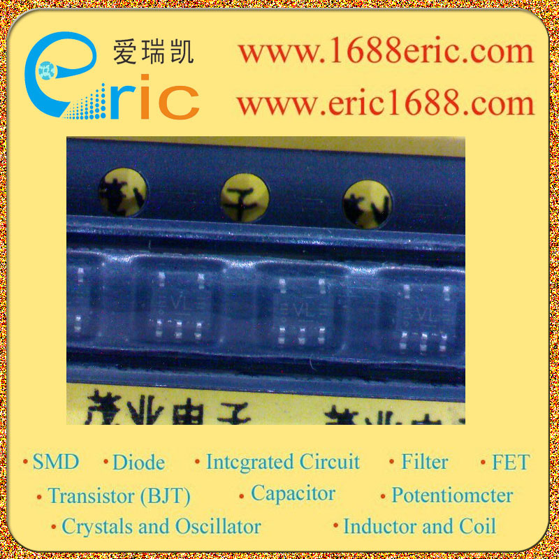
74LVC1G66GW VL 的参数 |
| 开关配置
Circuit |
单刀单掷 1*SPST |
| 导通电阻
On-State Resistance |
15Ω/Ohm |
| 电源电压
Voltage - Supply |
1.65V~5.5V |
| Description & Applications |
Bilateral switch The 74LVC1G66 provides one single pole, single-throw analog switch function. It has two input/output terminals (Y and Z) and an active HIGH enable input pin (E). When E is LOW, the analog switch is turned off. Schmitt-trigger action at the enable input makes the circuit tolerant of slower input rise and fall times across the entire VCC range from 1.65 V to 5.5 V. Wide supply voltage range from 1.65 V to 5.5 V Very low ON resistance: 7.5 ? (typical) at VCC = 2.7 V 6.5 ? (typical) at VCC = 3.3 V 6 ??(typical) at VCC = 5 V Switch current capability of 32 mA High noise immunity CMOS low power consumption TTL interface compatibility at 3.3 V Latch-up performance meets requirements of JESD78 Class I ESD protection: HBM JESD22-A114F exceeds 2000 V MM JESD22-A115-A exceeds 200 V Enable input accepts voltages up to 5.5 V Multiple package options Speci?ed from ?40 °C to +85 °C and ?40 °C to +125 °C |
| 描述与应用 |
双边开关 74LVC1G66提供一个单极单掷模拟开关的功能。它有两个 输入/输出端子(Y和Z)和主动高启动输入引脚(E)。当E为低, 模拟开关是关闭的。 在使能输入施密特触发动作使电路宽容输入上升较慢 下降时间在整个VCC范围从1.65 V至5.5 V。 ?从1.65 V至5.5 V的宽电源电压范围 ?非常低的导通电阻: ?7.5Ω VCC=2.7 V(典型值) ?6.5Ω?VCC= 3.3 V(典型值) ?6 Ω? VCC= 5 V(典型值) ?开关电流容量为32毫安 ?高抗干扰 ?CMOS低功耗 ?在3.3 V TTL接口的兼容性 ?闭锁性能符合JESD78类的要求,我 ?ESD保护: ?HBM JESD22-A114F超过2000 V ?MM JESD22-A115-A超过200 V ?允许接受输入电压高达5.5 V ?多种封装选项 从-40°C至+85°C和-40°C至+125°C |
| 技术文档PDF下载 |
在线阅读  |
|
|
|
|
|
相关型号列表 |
| 型号 |
标记/丝印/代码 |
厂家 |
批号 |
封装 |
数量 |
描述 |
详细资料 |
| 74LVC1G66GW |
VL |
NXP/PHILIPS |
07NOPB |
SOT-353/SC70-5 |
0 |
集成电路ICIntegrated Circuit(IC)-开关ICSwitch IC-模拟开关Analog Switch |
查看 |
|
|
|