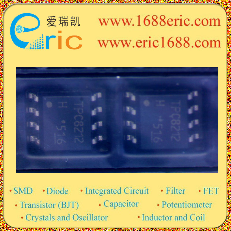
TPC8212 TPC8212 的参数 |
| 最大源漏极电压Vds
Drain-Source Voltage |
30V |
| 最大栅源极电压Vgs(±)
Gate-Source Voltage |
±20V |
| 最大漏极电流Id
Drain Current |
6A |
| 源漏极导通电阻Rds
Drain-Source On-State Resistance |
16mΩ~21mΩ VGS = 10 V , ID = 3 A |
| 开启电压Vgs(th)
Gate-Source Threshold Voltage |
1.1V~2.3V VDS = 10 V, ID = 1 mA |
| 耗散功率Pd
Power Dissipation |
0.75W |
| Description & Applications |
TOSHIBA Field Effect Transistor Silicon N-Channel MOS Type (Ultra-High-Speed U-MOSIII) .
* High-Efficiency DC/DC Converter Applications
* Notebook PC Applications
* Portable-Equipment Applications
* Small footprint due to small and thin package
* High-speed switching
* Small gate charge: QSW = 5.5 nC (typ.)
* Low drain-source ON-resistance: RDS (ON)= 16 mΩ (typ.)
* High forward transfer admittance: |Yfs| =14 S (typ.)
* Low leakage current: IDSS = 10 ??A (max) (VDS = 30 V)
* Enhancement mode: Vth = 1.1 to 2.3 V (VDS = 10 V, ID = 1 mA) |
| 描述与应用 |
东芝场效应晶体管的硅N沟道MOS型(超高速U-MOSIII),。
*高效率DC/ DC转换器应用
*笔记本电脑应用
*便携式设备应用
*由于占地面积小,小而薄的包装
*高速开关
*小门负责人:QSW= 5.5 NC(典型值)
*低漏源导通电阻RDS(ON)= 16mΩ(典型值)
*较强的正向转移导纳:| YFS|=14 S(典型值)
*低漏电流IDSS= 10μA(最大)(VDS=30 V)
*增强模式:VTH =1.1到2.3 V(VDS=10V,ID= 1 mA时) |
| 技术文档PDF下载 |
在线阅读  |