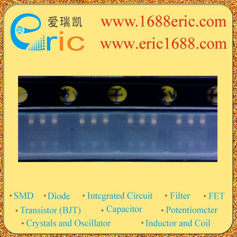
NDC7002N 02N �IJ��� |
| ���Դ©����ѹVds
Drain-Source Voltage |
50V |
| ���դԴ����ѹVgs(��)
Gate-Source Voltage |
20V |
| ���©������Id
Drain Current |
510mA/0.51A |
| Դ©����ͨ����Rds
Drain-Source On-State Resistance |
4?@ VGS =4.5V, ID =350mA |
| ������ѹVgs��th��
Gate-Source Threshold Voltage |
1~2.5V |
| ��ɢ����Pd
Power Dissipation |
960mW/0.96W |
| Description & Applications |
Dual N-Channel Enhancement Mode Field Effect Transistor General Description These dual N-Channel Enhancement Mode Field Effect Transistors are produced using Fairchild��s proprietary, high cell density, DMOS technology. This very high density process has been designed to minimize on-state resistance, provide rugged and reliable performance and fast switching. These device is particularly suited for low voltage, low current, switching, and power supply applications. Features ? High saturation current ? High density cell design for low RDS(ON) ? Proprietary SOT �C6 package: design using copper lead frame for superior thermal and electrical capabilities |
| ������Ӧ�� |
˫N������ǿ�ͳ�ЧӦ����� ���� ��Щ˫N������ǿ�ͳ�ЧӦ����ܶ����÷��װ뵼��ר�еģ���ϸ���ܶȣ�DMOS��������dz����ܶȹ�����ּ������ȵؼ���̬ͨ���裬�ṩ��̿ɿ������ܺͿ����л�������Щ�豸�ر��ʺ��ڵ͵�ѹ���͵��������أ���Դ�е�Ӧ�á� �ص� ?�߱��͵��� ?���ܶȵ����Ƶĵ�RDS��ON�� ?ר��SOT-6��װ��Ʋ���ͭ���߿�ܵ�Խ�Ⱥ͵������� |
| �����ĵ�PDF���� |
�����Ķ�  |