|
|
|
|
|
|
|
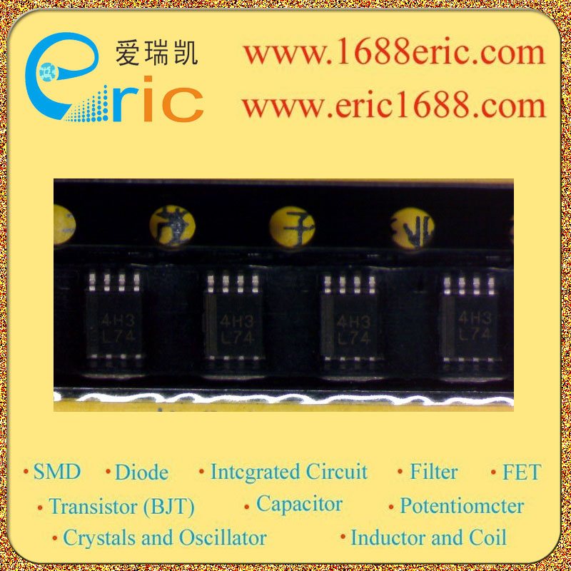
HD74LV2G74AUSE L74 �IJ��� |
| ����
Function |
���ã�Ԥ�裩��λ Set(Preset) and Reset |
| ����
Type |
D�� D-Type |
| �������
Output Type |
��� Differential |
| Ԫ����
Number of Elements |
1 |
| ÿԪ��λ��
Number of Bits per Element |
1 |
| ʱ��Ƶ��
Frequency - Clock |
20MHz |
| �����ӳ�ʱ��
Delay Time - Propagation |
1ns |
|
������ Positive Edge |
| ����������
Trigger Type |
12mA��12MA |
| ����ߵ�ƽ���͵�ƽ����
Current - Output High, Low |
-0.5-7.0V |
| ��Դ��ѹ
Voltage - Supply |
Single D�Ctype Flip Flops with Preset and Clear Description The HD74LV2GT74A has independent data, preset, clear, and clock inputs Q and Q outputs in an 8 pin package. The input data is transferred to the output at the rising edge of clock pulse CLK. The input protection circuitry on this device allows over voltage tolerance on the input, allowing the device to be used as a logic�Clevel translator from 3.0 V CMOS Logic to 5.0 V CMOS Logic or from 1.8 V CMOS logic to 3.0 V CMOS Logic while operating at the high-voltage power supply. Low voltage and high-speed operation is suitable for the battery powered products (e.g., notebook computers), and the low power consumption extends the battery life. Features ? The basic gate function is lined up as Renesas uni logic series. ? Supplied on emboss taping for high-speed automatic mounting. ? TTL compatible input level. Supply voltage range : 3.0 to 5.5 V Operating temperature range : �C40 to +85��C ? Logic-level translate function 3.0 V CMOS logic �� 5.0 V CMOS logic (@VCC = 5.0 V) 1.8 V or 2.5 V CMOS logic �� 3.3 V CMOS logic (@VCC = 3.3 V) ? All inputs VIH (Max.) = 5.5 V (@VCC = 0 V to 5.5 V) All outputs VO (Max.) = 5.5 V (@VCC = 0 V) ? Output current ��6 mA (@VCC = 3.0 V to 3.6 V), ��12 mA (@VCC = 4.5 V to 5.5 V) ? All the logical input has hysteresis voltage for the slow transition. ? Ordering Information |
| Description & Applications |
��·D�͵���������Ԥ�ú������� ���� ��HD74LV2G74A�ж��������ݣ�Ԥ�ã���������ʱ������Q��Q���һ��8���ŷ�װ���� �������ݱ�ת�Ƶ����ʱ������CLK�������ء��͵�ѹ������ת �������ɵ�ع���IJ�Ʒ����ʼDZ����ԣ����͵��ĵ����� ��ص������� �ص� ?�������Ź���һ���ſ�����Ϊ����������ϵ�С� ?�ṩ��������Զ���װ¼���� ���������൱��HD74LV74A ��Դ��ѹ��Χ��1.65��5.5 V �����¶ȷ�Χ��-40��+85��C ?��������VIH�����=5.5 V��VCC= 0 V��5.5 V�� �������VO�����=5.5 V��VCC=0 V�� ?���������6������VCC= 3.0 V��3.6 V������12������VCC= 4.5 V��5.5 V�� ?�������������ͺ��ѹ�Ļ������ɡ� ?������Ϣ |
| ������Ӧ�� |
|
| �����ĵ�PDF���� |
�����Ķ�  |
|
|
|
�� |
|
����ͺ��б� |
| �ͺ� |
���/˿ӡ/���� |
���� |
���� |
��װ |
���� |
���� |
��ϸ���� |
| HD74LV2G74AUSE |
L74 |
HITACHI |
05+ |
SSOP8 |
0 |
���ɵ�·ICIntegrated Circuit��IC��-����·Logic circuit-������Flip Flops |
�鿴 |
| HD74LV2G74AUSE |
L74 |
HITACHI |
05+ |
SSOP8 |
410 |
���ɵ�·ICIntegrated Circuit��IC�� |
�鿴 |
|
|
��
|