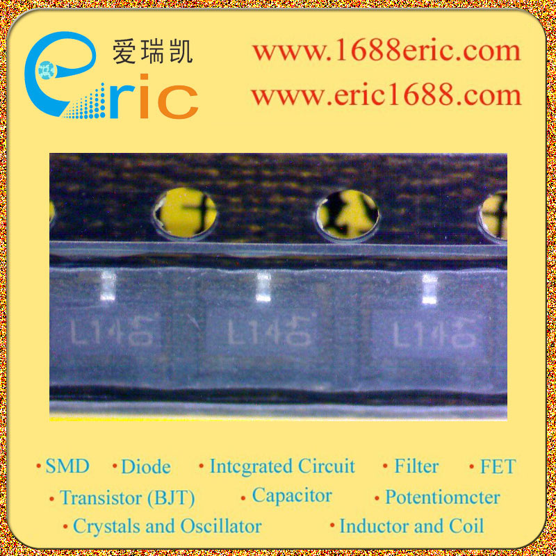
DTB114GK L14 өДІОКэ |
| јҜөзј«-»щј«·ҙПт»чҙ©өзС№V(BR)CBO
Collector-Base Voltage(VCBO) |
-50V |
| јҜөзј«-·ўЙдј«·ҙПт»чҙ©өзС№V(BR)CEO
Collector-Emitter Voltage(VCEO) |
-50V |
| јҜөзј«Б¬РшКдіцөзБчIC
Collector Current(IC) |
-500mA/0.5A |
| »щј«КдИлөзЧиR1
Input Resistance(R1) |
10KҰё/Ohm |
| »щј«-·ўЙдј«КдИлөзЧиR2
Base-Emitter Resistance(R2) |
|
| өзЧиұИ(R1/R2)
Resistance Ratio |
|
| ЦұБчөзБчФцТжhFE
DC Current Gain(hFE) |
56 |
| ҪШЦ№ЖөВКfT
Transtion Frequency(fT) |
200MHz |
| әДЙў№ҰВКPc
Power Dissipation |
0.2W/200mW |
| Description & Applications |
Features ??500mA / ?50V Digital transistors (with built-in resistors) ?The built-in bias resistors consist of thin-film resistors with complete isolation to allow positive biasing of the input, and parasitic effects are almost completely eliminated. ?Only the on / off conditions need to be set for operation, making the device design easy. ?Higher mounting densities can be achieved. Applications Inverter, Interface, Driver |
| ГиКцУлУҰУГ |
МШөг ?500әБ°І/-50VКэЧЦҫ§Ме№ЬЈЁДЪЦГөзЧиЈ© ?ДЪЦГЖ«ЦГөзЧиЧйіЙөДұЎДӨөзЧиЖчНкИ«ёфАлЈ¬??ФКРнХэЖ«С№КдИләНјДЙъР§УҰјёәхНкИ«МФМӯЎЈ ?Ц»УРҝӘ/№ШМхјюРиТӘЙиЦГІЩЧчЈ¬К№Ч°ЦГөДЙијЖИЭТЧЎЈ ?ёЯГЬ¶И°ІЧ°ҫНҝЙТФКөПЦЎЈ УҰУГ ДжұдЖчЈ¬ҪУҝЪЈ¬Зэ¶ҜіМРт |
| јјКхОДөөPDFПВФШ |
ФЪПЯФД¶Б  |