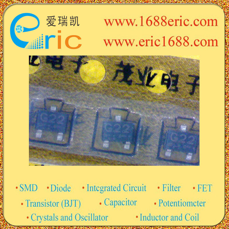
2SK2090 G22 的参数 |
| 最大源漏极电压Vds
Drain-Source Voltage |
50V |
| 最大栅源极电压Vgs(±)
Gate-Source Voltage |
7V |
| 最大漏极电流Id
Drain Current |
100mA/0.1A |
| 源漏极导通电阻ΩRds
DΩ/Ohmain-SouΩ/Ohmce On-State Ω/Ohmesistance |
15Ω/Ohm @10mA,4V |
| 开启电压Vgs(th)
Gate-Source Threshold Voltage |
0.7-1.5V |
| 耗散功率Pd
Power Dissipation |
150W |
| Description & Applications |
MOS FIELD EFFECT TRANSISTOR N-CHANNEL MOS FET FOR HIGH-SPEED SWITCHING The 2SK2090 is an N-channel vertical MOS FET. Because it can be driven by a voltage as low as 2.5 V and it is not necessary to consider a drive current, this FET is ideal as an actuator for low-current portable systems such as headphone stereos and video cameras. Features MOS FIELD EFFECT TRANSISTOR Gate can be driven by 2.5 V Because of its high input impedance, there’s no need to consider drive current |
| 描述与应用 |
MOS场效应晶体管 N沟道MOS FET高速开关 2SK2090是一个N沟道垂直MOS FET。因为 它可以由一个电压驱动低至2.5 V,这是不 必要考虑驱动电流,这FET是理想的作为 执行器的低电流的便携式系统,如耳机 音响和摄像机。 特性 MOS场效应晶体管 栅极可以由2.5 V驱动 由于其高输入阻抗就没有必要考虑驱动电流 |
| 技术文档PDF下载 |
在线阅读  |